Biden-Harris Administration reveals TSMC terms

The U.S. Department of Commerce and TSMC Arizona Corporation have signed a non-binding preliminary memorandum of terms (PMT) to provide up to $6.6 billion in direct funding under the CHIPS and Science Act.
This proposed funding would support TSMC’s investment of more than $65 billion in three greenfield leading-edge fabs in Phoenix, Arizona, which will manufacture the world’s most advanced semiconductors.
Through this proposed investment in TSMC Arizona, the Biden-Harris Administration would take a significant step in strengthening U.S. economic and national security by providing a reliable domestic supply of the chips that will underpin the future economy, powering the AI boom and other fast-growing industries like consumer electronics, automotive, Internet of Things, and high-performance computing. After initially announcing two fabs in the U.S., TSMC Arizona is committing to build an additional third fab before the end of the decade. With this proposed funding, TSMC Arizona would be ensuring the formation of a scaled leading-edge cluster in Arizona, creating approximately 6,000 direct manufacturing jobs, more than 20,000 accumulated unique construction jobs, and tens of thousands of indirect jobs in this decade and bringing the most advanced process technology to the United States.
“Semiconductors – those tiny chips smaller than the tip of your finger – power everything from smartphones to cars to satellites and weapons systems. America invented these chips, but over time, we went from producing nearly 40% of the world’s capacity to close to 10%, and none of the most advanced chips, exposing us to significant economic and national security vulnerabilities. I was determined to turn that around, and thanks to my CHIPS and Science Act – a key part of my Investing in America agenda – semiconductor manufacturing and jobs are making a comeback,” said President Joe Biden. “TSMC’s renewed commitment to the United States, and its investment in Arizona represent a broader story for semiconductor manufacturing that’s made in America and with the strong support of America’s leading technology firms to build the products we rely on every day.”
“One of the key goals of President Biden’s CHIPS and Science Act was to bring the most advanced chip manufacturing in the world to the U.S., and with this announcement and TSMC’s increased investment in their Arizona campus, we are working to achieve that goal,” said U.S. Secretary of Commerce Gina Raimondo. “The leading-edge semiconductors that will be made here in Arizona are foundational to the technology that will define global economic and national security in the 21st century, including AI and high-performance computing. Thanks to President Biden’s leadership and TSMC’s continued investments in U.S. semiconductor manufacturing, this proposed funding would help make our supply chains more secure and create thousands of good-quality construction and manufacturing jobs for Arizonans.”
“America’s ability to maintain our competitive edge in advanced technologies like artificial intelligence is essential to igniting the next generation of research, innovation, development, and production,” said Under Secretary of Commerce for Standards and Technology and National Institute of Standards and Technology Director Laurie E. Locascio. “Our proposed support for TSMC Arizona represents an inflection point for America’s innovative capacity that would restore our nation’s leadership in an industry that is foundational to the U.S. and global digital economy.”
“The proposed funding from the CHIPS and Science Act would provide TSMC the opportunity to make this unprecedented investment and to offer our foundry service of the most advanced manufacturing technologies in the United States,” said TSMC Chairman Dr. Mark Liu. “Our U.S. operations allow us to better support our U.S. customers, which include several of the world’s leading technology companies. Our U.S. operations will also expand our capability to trailblaze future advancements in semiconductor technology.”
“We are honored to support our customers who have been pioneers in mobile, artificial intelligence and high-performance computing, whether in chip design, hardware systems or software, algorithms, and large language models,” said TSMC CEO Dr. C.C. Wei. “They are the innovators driving demand for the most advanced silicon that TSMC can provide. As their foundry partner, we will help them unleash their innovations by increasing capacity for leading-edge technology through TSMC Arizona. We are thrilled by the progress of our Arizona site to date and are committed to its long-term success.”
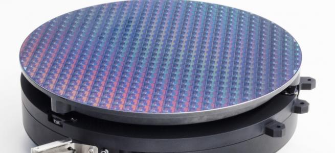
TSMC is widely recognized as a global leader in semiconductor manufacturing, having pioneered the pure-play foundry business model in 1987, and now manufactures over 90% of the world’s leading-edge logic chips. In Arizona, TSMC’s three fabs are expected to bring a suite of the most advanced process node technologies to the United States: the first fab will produce 4nm FinFET process technologies; today, TSMC Arizona announced that the second fab will produce the world’s most advanced 2nm nanosheet process technology, in addition to previously announced plans to produce 3nm process technologies; and TSMC Arizona’s third fab will produce 2nm or more advanced process technologies depending on customer demand. At full capacity, TSMC Arizona’s three fabs would manufacture tens of millions of leading-edge chips that will power products like 5G/6G smartphones, autonomous vehicles, and AI datacenter servers. TSMC Arizona expects to begin high-volume production in their first fab in the U.S. by the first half of 2025.
Thanks to investments like those at TSMC Arizona, the United States is now on track to produce roughly 20% of the world’s leading-edge chips by 2030. With total capital expenditures of more than $65 billion, TSMC Arizona’s investment is the largest foreign direct investment in a greenfield project in U.S. history. TSMC Arizona’s investment in the United States is catalyzing meaningful investment across the supply chain, including from 14 direct suppliers that plan to construct or expand plants in Arizona or other parts of the U.S., further strengthening U.S. domestic supply chain resilience.
TSMC’s advanced chips are the backbone of core processing units (“CPUs”) for servers in large-scale datacenters and of specialized graphic processing units (“GPUs”) used for machine learning. Through the proposed funding for TSMC Arizona, the United States would onshore the critical hardware manufacturing capabilities that underpin AI’s deep language learning algorithms and inferencing techniques. This would help strengthen America’s competitive edge in science and technology innovation. Furthermore, through its Arizona fabs, TSMC will be able to better support its key customers, including U.S. companies AMD, Apple, Nvidia, and Qualcomm, among others, by addressing their leading-edge capacity demand, mitigating supply chain concerns, and enabling them to compete effectively in the ongoing digital transformation era. With the proposed incentives, TSMC Arizona has also committed to support the development of advanced packaging capabilities – the next frontier of technology innovation for chip manufacturing – through its partners in the U.S., creating the opportunity for TSMC Arizona’s customers to be able to purchase advanced chips that are made entirely on U.S. soil.
The PMT also proposes $50 million in dedicated funding to develop the company’s semiconductor and construction workforce. To build the long-term construction workforce needed to support these projects, TSMC Arizona recently signed an agreement with the Arizona Building and Construction Trades Council. The company also plans to utilize registered apprenticeship programs to meet a 15 percent apprenticeship utilization rate on the Phoenix construction site.
As part of its commitment to developing local talent, TSMC Arizona established one of the first state-supported Registered Apprenticeship programs for semiconductor technicians, with support from the City of Phoenix. TSMC's U.S.-based recruiting team is also actively collaborating with university engineering programs around the country, including Arizona State University, University of Arizona, and Purdue University, and is partnering with Maricopa Community Colleges and career technical education programs on initiatives to develop the skills for a career in the semiconductor industry. Site employees have access to discounts, reimbursements, and priority enrollment through partnerships for local area early education and childcare centers.
In addition to the proposed direct funding of up to $6.6 billion, the CHIPS Program Office would make approximately $5 billion of proposed loans – which is part of the $75 billion in loan authority provided by the CHIPS and Science Act – available to TSMC Arizona under the PMT. The company has indicated that it is planning to claim the Department of the Treasury’s Investment Tax Credit, which is expected to be up to 25% of qualified capital expenditures.
As explained in its first Notice of Funding Opportunity, the Department may offer applicants a PMT on a non-binding basis after satisfactory completion of the merit review of a full application. The PMT outlines key terms for a potential CHIPS incentives award, including the amount and form of the award. The award amounts are subject to due diligence and negotiation of a long-form term sheet and award documents and are conditional on the achievement of certain milestones. After the PMT is signed, the Department begins a comprehensive due diligence process on the proposed projects and continues negotiating or refining certain terms with the applicant. The terms contained in the long-form term sheet and the final award documents may differ from the terms of the PMT being announced today.