Wafer-level Integration Changes of ALD for 2D Materials
Meeting the challenges of advanced process development for the
integration of ALD grown two-dimensional (2D) materials at wafer level.
Friedrich Witek, Senior Manager SENTECH Instruments
The “Research Laboratory Microelectronics Bochum for 2D Electronic Systems” (ForLab PICT2DES) project aims at attaining high-level applications in microelectronics and microsystems technology at a wafer level. The unique optical, thermal, and mechanical properties that exist in two-dimensional (2D) materials such as Transition-metal dichalcogenides (TMDs) have extremely promising applications in the growing areas of micro-technologies including highly-sensitive sensors, ultra-thin logic devices, nanogenerators, electronics, and optoelectronic devices. Although these materials pose some process challenges, the tunability of electrical and optical properties via the layer thickness of the 2D materials has great potential for future use cases. Ruhr-Universität Bochum (RUB) is working to establish a stable and scalable process chain, integrating additive and subtractive technologies with a high yield at a wafer level, that allows a transfer to industrial use. Working with the thinnest, 2D materials in electronics and sensors, 2D materials enable completely new, transparent, flexible, and biocompatible solutions with minimal consumption of resources.
BRIDGING THE GAP BETWEEN RESEARCH TO APPLICATIONS IN MICROELECTRONICS AND MICROSYSTEMS TECHNOLOGY AT A WAFER LEVEL WITH MOLYBDENUM DISULFIDE (MoS2) 2D MATERIALS
Establishing stable and scalable processes with a high yield at a wafer level using ultra-thin 2D materials creates several process challenges,
• High-quality, large-area monolayer precise growth at low processing temperatures
• Damage-free plasma deposition on 2D materials
• Homogeneous, monolayer precise, low damage, selective etching of 2D materials
• Electrical contacts
One of the key barriers to using 2D materials in an industrial environment is the growth of the material with similar stability, low defect density, and reliability compared to Silicon (Si). From an industrial point of view, avoiding the time and cost-intensive transfer processes of 2D materials is desirable, and therefore creates a demand for a bottom-up approach: direct deposition of high-quality 2D films on the target substrate. Due to the temperature sensitivity of the substrates, the bottom-up processes developed for 2D flexible electronics should have the lowest processing temperatures available. Thereby, a well-controlled and conformal growth of layer stacks including 2D materials on the wafer is mandatory. There is a need for dielectric integration with 2D materials for real devices and systems.
The band gap of many 2D materials as well as the transition from a direct to an indirect band structure depend on the number of layers. Thus, a homogeneous monolayer-precise deposition technology, without affecting the underlying layer is crucial but very challenging.
Since MoS2 has no chemical bonds on the surface, it cannot bond with metal, leading to a high Schottky barrier and low carrier injection efficiency. MoS2 has two different stable phases, a metallic 1T phase, and the semiconducting 2H phase, and thus new lateral phase-change contacts can be successfully demonstrated on flakes on a laboratory scale but need to be shown on a wafer scale.

PROJECT REQUIREMENTS
A cost-effective, innovative, monolayer-accurate deposition, etching, and fabrication technology needed to be implemented. The manufacturing processes for flexible microelectronics and ultra-sensitive micro sensors needed to work at low temperatures and be scalable towards a 200 mm wafer technology. Furthermore, the system needed to be compatible with both the Research Fab Microelectronics Germany (FMD) and industrial users.
MEETING THE PROJECT REQUIREMENTS
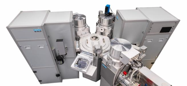
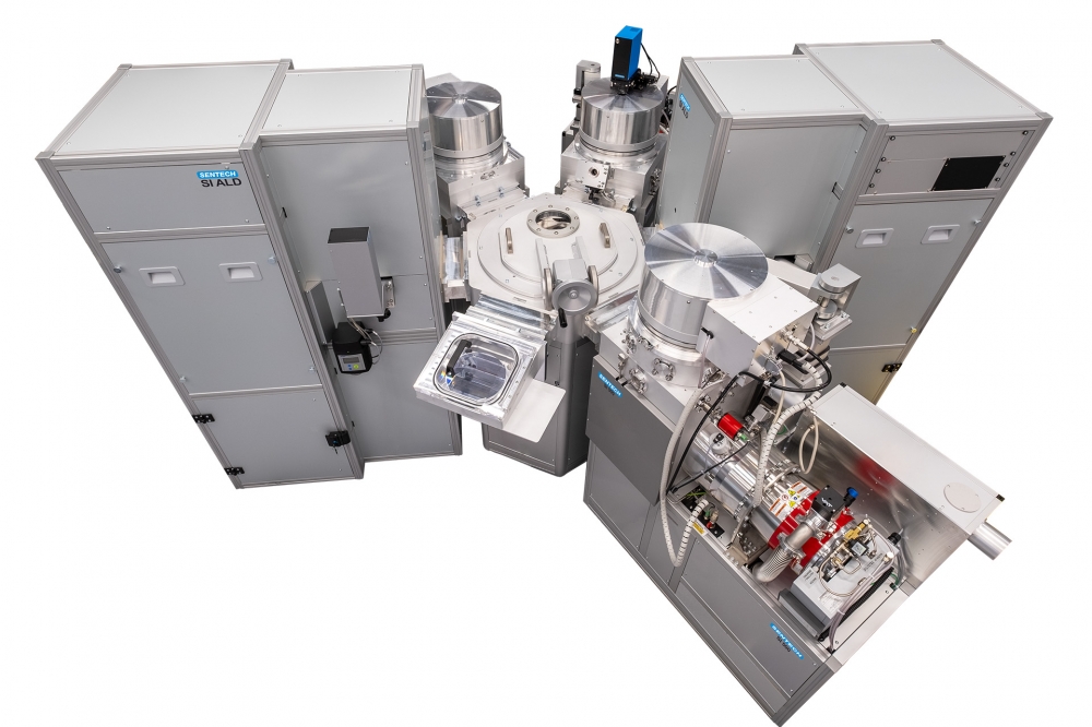
The ultra-thin 2D films are sensitive to environmental humidity and oxygen. To avoid degradation during sample transfer there was a requirement for a large cluster tool with direct encapsulation for the growth of the 2D materials, without breaking the vacuum. Due to the aim of scaling up to wafer level, the tool needed to study the performance of mass production techniques, wafer-to-wafer uniformity, homogeneity, and reproducibility, plus monolayer atomic layer deposition (ALD) growth. Following an open commercial tender process, the cluster tool from SENTECH Instruments (Figure 1) was chosen. This solution provides excellent modules for each process type, plasma enhanced atomic layer etching (PEALE), inductively coupled plasma-enhanced chemical vacuum deposition (ICPECVD), inductively coupled plasma-reactive ion etching (ICP-RIE), and plasma-enhanced atomic layer deposition (PEALD). For the latter one, a SENTECH True Remote Conductively Coupled Plasma (CCP) Source is used, allowing low-damage deposition of 2D materials. Another key factor is the SENTECH Planar Triple Spiral Antenna (PTSA) ICP source, enabling low-damage processing of 2D materials after their deposition. The individual tools offer port access for all of the plasma diagnostics required by the Chair of Applied Plasma Dynamics and Electrical Engineering (AEPT). The in-situ ALD and atomic layer etching (ALE) monitoring systems allow excellent control of the monolayer deposition and etching of the 2D materials during the entire process. A high level of customisation was required, which the experienced, interdisciplinary SENTECH project team was able to fulfil in conjunction with the transdisciplinary team at RUB.
PROCESS INTEGRATION USING THE CLUSTER TOOL
The process steps:
• Substrate pre-treatment
• High-k dielectric (ALD)
• Second substrate pre-treatment
• Monolayer precise deposition of the 2D material
• Surface passivation and passivation layer,
could all be carried out completely under vacuum, resulting in extremely clean surfaces, crucial for proper interfaces within the device. For process steps occurring outside of the vacuum, devices are passivated by a protective encapsulation film and metallisation, so it is possible to avoid a complete degradation of the 2D ultra-thin film.
KEY OBJECTIVES FOR PLASMA PROCESSING
The key factors needed in the plasma processing were:
• Compatibility with common device materials
• High level of control
• Capable of patterning at high resolution without altering the physical, electronic, and optical properties of the 2D devices, i.e., no-damage processing.
A plasma surface modification, a substrate pre-treatment, a monolayer precise ablation, and only a monolayer precise deposition were required. In all cases, precise control of the plasma properties was mandatory, thus the requirement for the custom plasma diagnostic rings (Figure 2), which were introduced within both the RIE chamber, used for fluorine gasses, and also in the ALE chamber. The rings are removable, which means that they can be replaced with a conventional spacer ring, allowing for a comparison of processes and transfer to any RIE system. They also allow the use of different plasma diagnostic tools, such as a retarding field energy analyser sensor array to determine, ion energies distribution functions and ion flux. Furthermore, optical emission spectroscopy was utilised to get information about the plasma composition.
SUPPORTING THE COMPLEX CLUSTER TOOL INFRASTRUCTURE CONFIGURATION
A great deal of preplanning was required due to the complex and interdisciplinary nature of the project and the integrated cluster tool. All stakeholders worked together, to ensure minimal complications and downtime from delivery, installation, and uptime of the equipment. The configuration of the cluster tool was complex and thus, supporting the infrastructure as a university was a major challenge. The cluster tool required 14 process gas lines, 42 process gas inlets, and around 300 metres of stainless-steel pipework for the gas supply, mainly within the cluster but also for on-site installation, this had to be housed within one room (Figure 3). The cluster tool and its additional equipment, including gas supply and waste gas management, had to be fully integrated into the safety infrastructure of the cleanroom due to the potentially hazardous nature of Cl-based gases, H2S, and Silane as well as highly-flammable and toxic ALD precursors. As an extra layer to the project, a waste gas purification plant (a dry bed absorber as a triple column system) needed an additional publication of a call for tenders. This needed to be completed relatively quickly to ensure it met the same timeline as the rest of the machinery.

The customer-specific modifications to the cluster tool took just under a year of interdisciplinary planning discussions between the SENTECH Application Team, Engineering, Technical Service, and experts from RUB. However, due to the scale and complexity of the tool and required infrastructure, the pre-planning proved invaluable in achieving the project goals within the required timescale. Working in close partnership ensured the machine configuration, infrastructure, and the questions concerning the compatibility and implementation of the gas sensor security system with the new equipment were all planned for well in advance.
The integrated cluster tool avoids cross-contamination, undesired doping, and exposure to humid environmental conditions, enabling enhanced film quality. Since March 2022 the tool has been working and initial results are very promising. Future collaborations and adaptations of the system are planned as part of the joint work of the BMBF-funded ForMikro project FlexTMDSense - “Research into a novel, flexible sensor systems based on two-dimensional material systems”. Research subjects include ultra-thin pH and gas sensor systems based on 2D Semiconductor Films from the material class of TMDs.
For further information about the cluster tool and bespoke plasma diagnostic ring, the process sequence, and the initial results for this project, it is possible to request a copy of a full case study. Please visit www.sentech.com and follow the links in the news section on the home page.
ABOUT RUHR-UNIVERSITÄT BOCHUM (RUB)
Located in the Ruhrgebiet, Ruhr-Universität Bochum (RUB) has 21 faculties and is home to over 42,600 students from countries all over the world. RUB is well-known as a top international scientific research institution, and is one of 12 “Research Laboratories in Microelectronics Germany” (ForLab) funded by BMBF. The ForLab project is designed to open up new research fields for microelectronics and act as a transition hub from science to industry.
ABOUT SENTECH Instruments GmbH
SENTECH Instruments develops, manufactures, and sells innovative equipment focused on deposition, structuring, and characterisation of thin films in Semiconductor Technology, Microsystems, Photovoltaics, Nanotechnology, and Materials Research. SENTECH offers advanced solutions for non-contact, non-invasive optical characterisation using Ellipsometry and Reflectometry. SENTECH is an expert in the ALE and ALD of thin films using plasma process technology, which supports many leading-edge applications.